
Prevent Signal Loss in PCB Fabrication Assembly
The integrity of signals passing through a PCB requires careful attention to design details, including the choice of component placement and routing. A structured design workflow that incorporates schematic design, PCB layout, and rigorous verification steps ensures the quality of the finished product. However, a poor design can cause a wide range of issues that can derail the assembly process and result in faulty final products. Signal integrity, electromagnetic compatibility, and thermal management are among the most common issues that can impact the quality of a PCB.
The skin effect, dielectric loss, and conductor loss all contribute to signal attenuation, which is the reduction in signal strength due to signal transmission through a conductor. This is particularly significant for high-speed digital signals. PCB designers can reduce attenuation by selecting low-loss materials/substrates, designing traces with proper width and length, and routing them close to ground planes, which can also help mitigate other types of losses like parasitic capacitance and impedance mismatch.
High-speed digital and analog signals require precise control of impedance to avoid unwanted reflections and jitter. These issues arise when a signal’s impedance doesn’t match the impedance of the source and load. To prevent them, designers must identify critical signals and use techniques like differential signaling to minimize the impact of impedance mismatches.
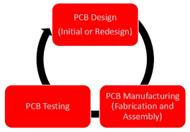
How to Prevent Signal Loss in PCB Fabrication Assembly
Other factors that can affect signal integrity include copper surface roughness, stray trace capacitance, and impedance mismatches between different layers of the board. In addition, the fabricator must ensure that there is adequate mechanical support between copper layers and the prepreg and resin. The high temperature and pressure that are applied during the fabrication process can also cause moisture absorption, which weakens the binding between the substrate layers. Moisture absorption can be prevented by following a rigorous fabrication process and providing detailed Gerber files that are free of acid traps.
PCB designers must also consider the effect of heat on signal integrity when implementing complex circuits. When a circuit is operating at high frequencies, the copper surface can become conductive and generate heat that will interfere with signal transmission. This can be avoided by incorporating heat dissipating features such as guard rings and ground pours, placing ICs in a separate circuit area, and using decoupling capacitors.
Lastly, PCB designers must take into account the effect of board thickness on signal integrity when determining which components to select and how to route them. Thick boards can increase loss through the insulating layer between copper layers, which can limit the amount of available current. This can be avoided by utilizing smaller components and arranging them strategically on the board to minimize thickness.
The best way to prevent signal loss is to implement careful design and fabrication processes, ensuring that all aspects of the design are optimized for manufacturability. This includes ensuring that all necessary layers are included in the Gerber file, providing accurate dimensions and tolerances, and adherence to manufacturability guidelines. In addition, pcb fabrication assembly designers should always carefully review the final prototype before submitting it for production to verify that the design is correct and will produce a dependable product.