
Ceramic Printed Circuit Boards More Expensive
Ceramic PCBs are an excellent choice for applications that require high thermal conductivity, low coefficient of thermal expansion (CTE), and chemical erosion resistance. They are also durable and can withstand extreme temperatures, making them the ideal substrate for high-heat devices like processors and motors. However, there are some important factors to consider before purchasing a ceramic circuit board, such as the materials used and the fabrication process. In this article, we’ll discuss the cost differences between alumina-, aluminum nitride-, and beryllium oxide-based ceramic PCBs.
One of the primary costs of ceramic PCBs is the raw material used in the substrate layer. Most manufacturers use alumina, aluminum nitride, or beryllium oxide as their base substrates. These materials have exceptional mechanical strength and electrical insulation properties, but they are more expensive than traditional PCB substrates like FR-4. Additionally, the manufacturing process used for these types of ceramic PCBs can be more labor intensive than other types.
The other main cost factor of ceramic printed circuit board is the conductive materials. The conductive traces are applied using metal pastes, which are then fused into the substrate using a heat and pressure process called sintering. During the sintering process, the ceramic absorbs and bonds with the metallic particles in the conductive material to form a strong and stable circuit structure. This allows the fabricator to put electrical components such as conductive and non-conductive layers, resistors, electric capacitors, and integrated circuits directly on the ceramic substrate without having to add an additional insulating layer. The conductive layers are then connected to each other via holes, or vias, that are drilled into the ceramic with laser or mechanical drilling techniques.
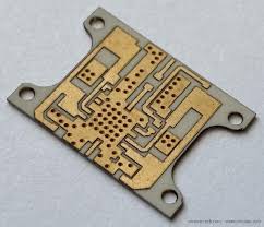
Are Ceramic Printed Circuit Boards More Expensive?
After the conductive materials have been bonded to the substrate, the fabricator can print the circuit pattern on the metal foil with photo-lithographic techniques and then apply a tin-lead resist layer to protect the unprotected areas. Then the fabricator can use a medium or small power RF CO2 laser to drill the via holes with high speed, accuracy, and efficiency. The via holes are then filled with conductive and non-conductive materials to establish connections between layers.
Some ceramic PCBs are made with silver traces, while others are plated with gold. Gold-plated traces are more expensive, but they offer superior electrical performance and connectivity to other components. Moreover, they can be soldered in places where silver corrosion might occur due to salts and chemicals. In addition, the ceramic PCBs with a thin-plate structure are better for etching different layouts and can fit into compact spaces. They are typically finished with OSP, HASL, and Pb-free HASL surface finishes to increase their operational temperature range and improve corrosion resistance.