
HDI printed circuit board improve electrical performance
As consumer demand for smaller and more powerful electronic devices increases, manufacturers sought a way to increase component density without sacrificing electrical performance. This led to innovations such as HDI printed circuit boards, which feature smaller components and advanced design techniques. However, the increased component density can also create more complex electrical circuits that require more precise routing and finer traces to ensure optimal function. In this article, we explore how an HDI PCB can improve electrical performance through tighter spacing and shorter pathways for signals.
Increasing the number of layers in a PCB requires more careful design and manufacturing processes. This can lead to higher costs and longer production times for the final product. However, the higher reliability and improved performance of HDI PCBs more than offset these added costs. In addition, the ability to place more components on a single PCB can allow for the development of new and innovative products that could not be made with traditional technology.
The primary advantage of an hdi printed circuit board is that it can offer shorter paths for electrical signals to travel. This reduces signal crossing delays and minimizes electromagnetic interference between adjacent traces and components. This reduced pathway length can be especially helpful in high-speed applications where every microsecond counts.
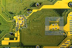
How does an HDI printed circuit board improve electrical performance?
In addition, the thinner dielectric material used in an HDI PCB allows for a lower signal loss and more efficient transmission than a standard PCB. This can be especially important in RF applications where the speed of signal transmission is essential for effective operation.
Additionally, HDI PCBs are designed to use finer traces and pads to accommodate the high-density layouts needed for these types of applications. This allows the designer to implement more precise routing and finer connections between the pads and traces. It also enables the use of smaller vias, known as microvias, which can significantly improve the overall quality of the signal.
The shortening of the signal path allows for better EMI management as well. The reduced distance between components also helps to keep the signal from resonating in the metal traces and causing interference. Adding ground planes or shields can further help to minimize interference by acting as quiet guardians to the signals on a PCB.
Lastly, HDI PCBs often incorporate thermal vias to efficiently manage heat dissipation. The thermal vias conduct the heat from hot-generating components to a cooling layer or external heat sink, which effectively cools the components and prevents them from overheating.
Choosing the correct materials for an HDI PCB is vital to ensure optimal electrical and thermal performance. The designer must consider the CTE value, performance under stress, and dielectric constant of each individual layer to choose a material that will best suit the application. It is also essential to carefully plan the stack-up for each layer of the circuit board. This includes choosing the right combination of through-vias and blind/buried vias. Lastly, the designer should avoid using staggered vias or Extra-Large Inner Connects (ELIC) unless absolutely necessary to preserve space on the board.